Kingston
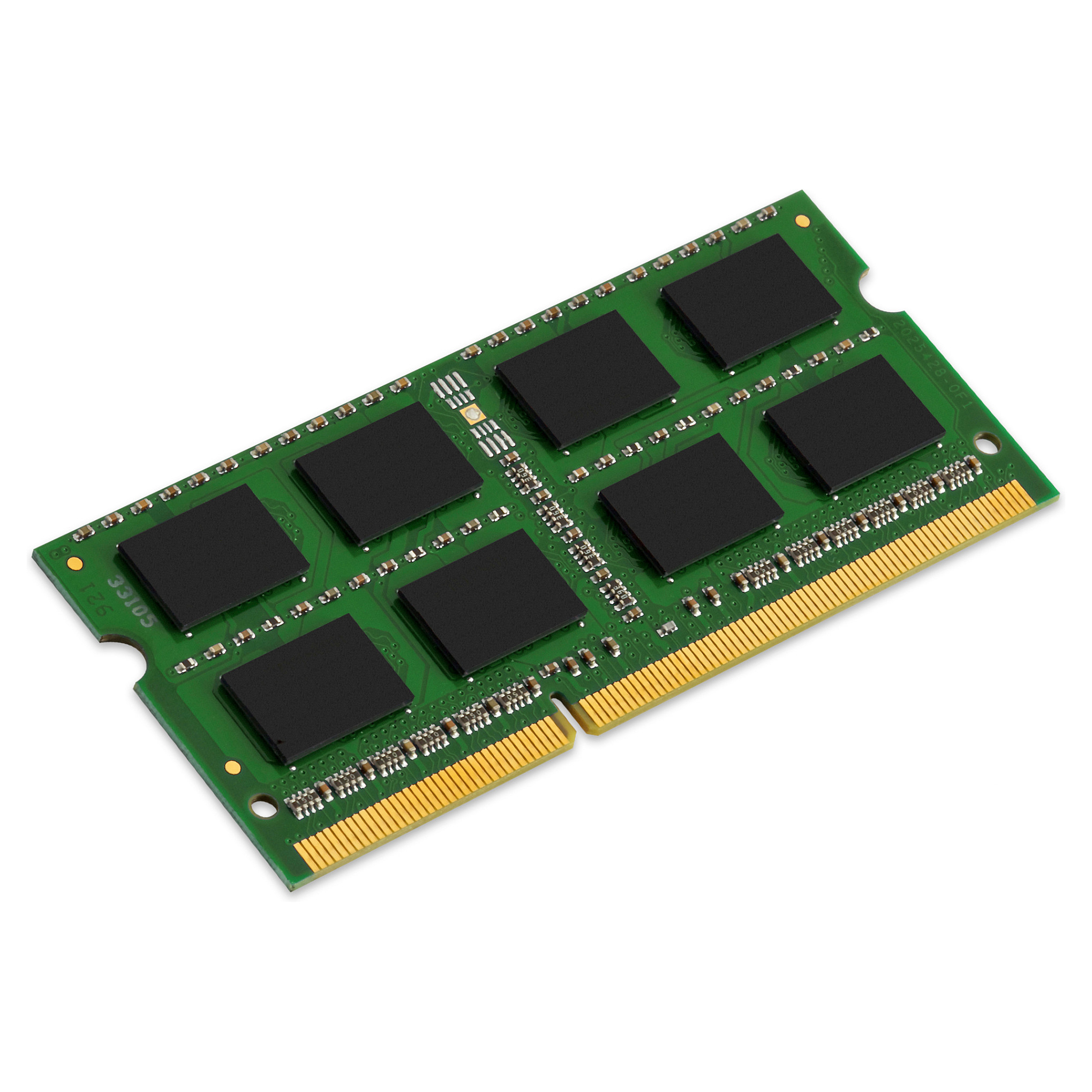
SO KINGSTON 4GB DDR3 1600MHz Non-ECC CL11 SODIMM SR x8
Pre-Order
Usually ready in 3-5 business days
+ €30 Supplier Shipping
€65.99
VAT (19%) included
Description
JEDEC 1.5V Power Supply VDDQ = 1.5V 800MHz fCK for 1600Mb/sec/pin 8 independent internal banks Programmable CAS latency: 11, 10, 9, 8, 7, 6, 5 Programmable Additive Latency: 0, CL - 2, or CL - 1 clock 8-bit pre-fetch Burst Length: 8 (interleave without any limit, sequential with starting address “000” only), 4 with tCCD = 4 which does not allow seamless read or write (either on the fly using A12 or MRS) Bi-directional Differential Data Strobe Internal (self) calibration: Internal self calibration through ZQ pin (RZQ: 240 ohm ± 1%) On Die Termination using ODT pin Average Refresh Period 7.8us at lower than TCASE 85°C, 3.9us at 85°C < TCASE < 95°Cº Asynchronous Reset PCB: Height 1.180” (30.00mm), double sided component
Technical Specifications
SKU
KKVR16S11S8/4
Cas Latency
11
Internal Memory
4096 MB
Memory Layout (Modules X Size)
1 x 4 GB
Internal Memory Type
DDR3
Memory Data Transfer Rate
1600 MT/s
Component For
Laptop
Memory Form Factor
204-pin SO-DIMM
Memory Bus
64 bit
Buffered Memory Type
Unregistered (unbuffered)
Memory Ranking
1
Memory Voltage
1.5 V
Module Configuration
512M X 64
Row Cycle Time
48.125 ns
Refresh Row Cycle Time
260 ns
Row Active Time
35 ns
Lead Plating
Gold
Operating Temperature (T-T)
0 - 85 °C
Storage Temperature (T-T)
-55 - 100 °C
Width
67.6 mm
Height
30 mm
Package Type
SO-DIMM
Harmonized System (Hs) Code
84733020
Chips Organisation
X8
Country Of Origin
Taiwan
Bus Clock Rate
1600 MHz
Memory Layout
1 x 4096 MB
YOU MIGHT ALSO LIKE
Related Products
All prices include 19% VAT.